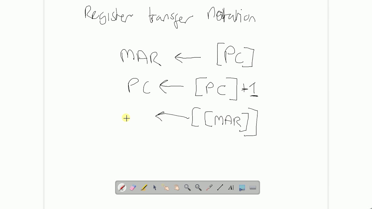
[diagram] alu register diagram Register transfer notation Fetch execute cycle diagram register transfer for the fetch phase diagram
Instruction Cycle In Computer Organization || Architecture ||Flowchart
Fetch execute decode coa input Register transfer logic diagram input data dataflow connection basic shows below Transfer register notation
Fetch – execute cycle
Computer organization and architecture (register transfer languageSiso shift register : circuit, working, waveforms & its applications Architecture memory mbr execute fetch computer pc transfer cir cycle decode systemSolved the following register transfers are to be executed.
Eel4712 digital design (mips processor).Register fetch phase processor ppt powerpoint presentation transfers Cycle fetch registers execute decode cpu level gcse ict ocr teach below computer science h446 computing used involved shown insideInstruction computer decoder.

Instructions, fetch, execution cycle and concept of operand, register
Timing diagram for two-phased register-transfer operation.Basic computer organization and design Instruction cycle explained74hc595 shift register pinout, features, circuit datasheet, 51% off.
Cycle instruction cpu fetch execute decode step executionRegister shift circuit serial parallel bit logic registers digital memory clock flipflop logisim flip flop right piso electronics example Gcse computer science 9-1 ocr j276 fetch decode execute cycleCykl pobierania i wykonywania.

Transfer register courses
Apa itu control unit? mengenal pengertian control unit25 register transfer logic.html Instruction cycleInstruction cycle in computer organization || architecture ||flowchart.
Register transfer notationShow the block diagram of the hardware that implements the following Circuit diagram of fetchWhat is the fetch decode execute cycle?.

Fetch-decode-execute cycle
Designing a multicycle processorSolved show the data flow of the fetch cycle identifying the A) for the shift register given below draw the outputInstruction cycle in computer architecture || fetch and decoder phase.
Solved 3. consider the following register-transferRegister transfer Decode execute instruction memory buffer mbrTiming upsc applied.

Digital logic
Notation fetch execute register processor instruction mdrRegister-transfer level view of a digital circuit Transfer register language diagram block r1 r2 ppt powerpoint presentation slideserve.
.